An upcoming Japanese bonding technology will enable the 5G Smart City revolution, believes Alex Spatzig, Business Development Manager for Mitsubishi Heavy Industries, Europe.
Nearly a hundred years on from the first commercial mobile telephony service – which, curiously enough, was offered on trains between Hamburg and Berlin in Germany – we are ushering in the fifth generation of mobile network technology, or 5G.
Each mobile generation has brought us new advances, from text messaging and apps to video calling and satellite navigation. And 5G is expected to take this to the next level: by enabling real-time services for smart cities as well as far-reaching industrial automation. Compared to 4G, it will be about 10 times faster, with speeds higher than 1 Gbps, compared to 4G’s 23-35 Mbps.
To achieve both these high data transmission speeds and low-latency connections, 5G uses radio waves with much higher frequencies and requires far more accurate signals than previous mobile generations. This poses a significant challenge for those involved in making 5G chips for mobile handsets.
The radio frequency filters in mobile handsets, especially surface acoustic wave (SAW) filters ensure that only exact frequencies are transmitted. However, achieving this level of filtering accuracy is hampered by some of the production methods currently used.
Bonding
Here is where Mitsubishi Heavy Industries’ (MHI) room-temperature bonding comes in. Thanks to its competitive features, such as high bonding strength, MHI room-temperature bonding is attracting the most industry attention among approximately ten established bonding methods, such as eutectic bonding or fusion bonding.
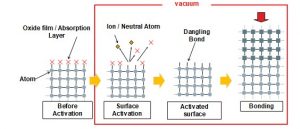
The key to MHI’s room-temperature bonding technique is to remove the native oxide film on the surface of the wafer by using an ion gun or FAB gun, which will result in free bonds (dangling bonds). These free bonds will then be used to connect with another wafer. In essence, this is surface-activated bonding (SAB), where two wafers bond because their surfaces have been chemically ‘activated’. The image below shows the principle behind MHI’s SAB process.
Principle of Room-Temperature Bonding (SAB). (Mitsubishi Heavy Industries)
Mastering this challenge in a viable manner could come down to a solution developed and standardized nearly 20 years ago at the University of Tokyo by Professor Tadatomo Suga, whose research greatly expanded the application field of room-temperature bonding.
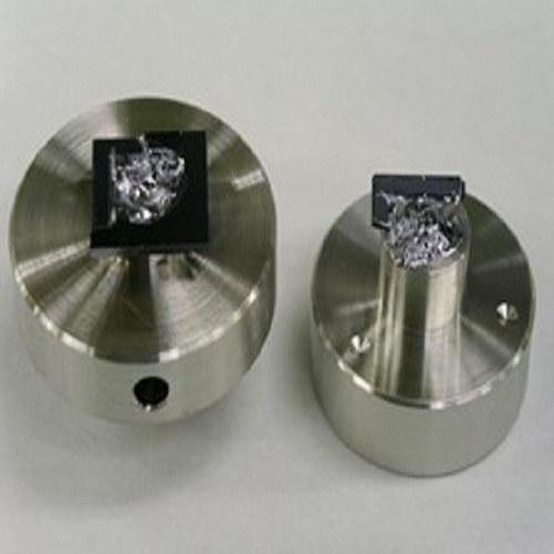
Not only does surface-activated bonding eliminate heat distortion, but it also has other advantages: the bonding strength is comparable to the mechanical strength of bulk material. In the pull test for the Si-Si bonding, which is shown in the picture below, its strength is equal to the bulk material.
Example: Si-Si bonding, pull test result, broken at base material (Mitsubishi Heavy Industries)
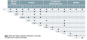
What’s more, room-temperature bonding works with a wide range of materials including those in the silicon family, oxides, compound semiconductors and metals.
Applicable materials of the MHI Room-Temperature Bonding. (Mitsubishi Heavy Industries)
The MHI room-temperature process also increases the yield rate through a shorter cycle time without the need for a heating-cooling cycle.
The MHI room-temperature bonding process is already being used in mass production of 5G devices by one of MHI’s business partners: D-Process, who is the foundry of CMP (Chemical Mechanical Polishing) and wafer bonding. Also, another SAW filter supplier in Japan and China have started the mass production of the device utilizing room-temperature bonding.
The reason that the SAW filter for the 5G devices needs to be bonded at room temperature is the Lithium Tantalate (LT: LiTaO3) substrate being used. The LT substrate is formed into a comb electrode to fulfil its main function: frequency filtering. The heat ultimately reduces the accuracy of the filter. In the worst case, a handset could end up transmitting on an entirely different frequency.
The problem is that heat is detrimental to the integrity of the LT substrate used for filtering. However, the most common technique for making SAW filters involves applying heat to bond together filter material and support material, such as silicon and sapphire wafers.
The support materials mentioned above are applied to forcibly suppress the thermal expansion of the LT substrate when the device gets hot after using it for a period of time, since silicon and sapphire have thermal expansion coefficients of about 1/5 relative to Lithium Tantalate. Also because of this huge difference in thermal expansion, the wafers would bend or break if bonded by heating. So the room-temperature option is the only choice for manufacturers.
SAB
Intriguingly, SAB technology has a wide range of applications beyond mobile phones and can already be found in MEMS (Micro Electric Mechanical Systems) such as automobile sensors and healthcare equipment.
Some other devices based on compound semiconductors like LED and power devices, which are currently bonded by conventional processes, are increasingly shifting to room-temperature bonding.
At the moment, these devices are largely being produced by a method called fusion bonding, in which O-H groups are formed by applying a plasma surface. When using this method, a highly hygroscopic film has to be applied to prevent voids. To get rid of this unwanted insulating layer, room-temperature bonding is a better choice, since the atoms are directly bonded with nothing in between.
But 5G will see SAB come truly into its own. Despite the pandemic, the worldwide 5G infrastructure market is expected to have nearly doubled in 2020, reaching more than $8 billion, according to industry analyst Gartner. Shipments of 5G-enabled smartphones were set to have grown to nearly 280 million units, mainly driven by high demand in China. By 2028, experts expect the overall 5G market to reach over $3 trillion.
As 5G networks proliferate, and smart services using 5G’s high-speed connectivity are widely adopted, room-temperature bonding looks set to be perfectly positioned to take advantage.
Source: electronicsweekly


