In the future, decarbonized societies that use internet of things (IoT) devices will become commonplace. But to achieve this, we need to first realize highly efficient and stable sources of renewable energy. Solar cells are considered a promising option, but their electrical contacts suffer from a “tradeoff” relationship between surface passivation and conductivity. Recently, researchers from Japan have developed a new type of electrical contact that can overcome this problem.

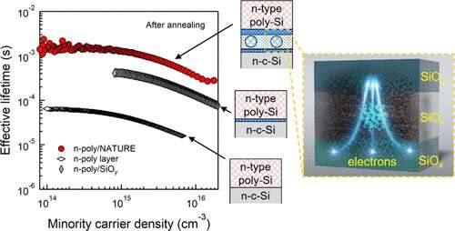
In a new study, published in ACS Applied Nano Materials, a research team led by Assistant Professor Kazuhiro Gotoh and Professor Noritaka Usami from Nagoya University has developed a novel SiOx layer that simultaneously allows high passivation and improved conductivity. Named NAnocrystalling Transport path in Ultrathin dielectrics for REinforcing passivating contact (NATURE contact), the new electrical contact consists of three-layer structures made up of a layer of silicon nanoparticles sandwiched between two layers of oxygen-rich SiOx. “You can think of a passivating film as a big wall with gates in it. In the NATURE contact, the big wall is the SiOx layer and the gates are Si nanocrystals,” explains Dr. Gotoh.
The conductivity of the electrical contact in solar cells is dependent on the formation of a “carrier pathway” for the transport of electronic charges. The formation of this electrical pathway is dependent upon a high temperature treatment called “annealing.”
Previous research has shown that SiOx contacts that contain silicon nanoparticles as a carrier pathway can achieve good electrical properties. In the NATURE contact, the annealing process leads to the formation of very small silicon nanocrystals in the passivation layer that are nearly spherical in shape. The diameter of these nanocrystals corresponds to the thickness of the passivation layer. Thus, by controlling the annealing conditions, the diameter and subsequent thickness of the passivation layer can be adjusted.
The research team fabricated NATURE contacts and then subjected them to varying annealing conditions. Upon studying the contacts with transmission electron microscopy, they discovered that silicon nanocrystals were formed in the contact at an annealing temperature of 750 °C. They also investigated the electrical properties of the contact. They saw that compared to existing contacts such as the tunnel oxide passivating contact (TOPCon) or polysilicon on the oxide (POLO) contacts, the NATURE had comparable values of contact resistance and “recombination current,”—a phenomenon that causes current and voltage losses in solar cells and decreases their efficiency.
“The NATURE contact overcomes the trade-off relationship between the protective ability and conductivity of passivating films. This development will lead to the realization of future building-integrated photovoltaics (BIPV) and vehicle-integrated photovoltaics (VIPV) and help us achieve zero-energy buildings and solar cars in future decarbonized societies,” concludes Dr. Gotoh.
Techxplore


