Scientist Develop World’s Thinnest Optical Waveguide. In today’s world of optical devices, thinner and smaller is better. The purpose of tinier devices is to create integrated photonic chips that can be shrunk down to the size of the integrated circuits (ICs) that are used in computer chips. The expectation is that miniaturization of optical devices will ultimately lead to higher density and higher capacity photonic chips.
In this drive towards thinner and smaller in optical devices, optical waveguides—a key component in optical data communications systems—have remained a stubborn nut to crack.
Now researchers at the University of California San Diego have developed an optical waveguide that consists of just three layers of atoms. This means that the new waveguide is just six angstroms thick. With one nanometer equal to 10 angstroms, and today’s optical waveguides typically around 200-300 nm, that means these new waveguides are 500 times thinner than what’s in use today.
“This might potentially lead to a higher density of waveguides or optical elements on an optoelectronic chip,” said Ertugrul Cubukcu, associate professor at UC San Diego. “Think about how a smaller transistor leads to a higher density of those on an electronic chip.”
To reach what is the theoretical limit in the thinness of an optical waveguide the researchers turned to transition metal dichalcogenides (TMDs), specifically tungsten disulfide.

TMDs are materials that combine one of 15 transition metals with one of three members of the chalcogen family: sulfur, selenium, or tellurium. Five years ago, simulations indicated that these materials could enable the thinning of the channel gates in transistors to below 1 nanometer.
The thinness of tungsten disulfide crystal is just one of the special properties of the material. The monolayer crystal also supports the formation of electron-hole pairs—also known as excitons—at room temperature.
In addition to operating at room temperature, tungsten disulfide can channel light in the visible spectrum. Graphene has been shown to serve as a waveguide. However, it can only operate at infrared wavelengths. This device serves as the first time that a material this thin can operate in the visible wavelengths.
Of course, actually trying to fashion a device out of a material only three-atoms thick may have been the largest hurdle of all for the researchers. “While these materials are very robust, macroscopic forces could have still damaged them,” explained Cubukcu.
In the research described in the journal Nature Nanotechnology, the researchers devised a way to handle this fragility by making use of a sacrificial template that was removed at the very last stage of the processing.
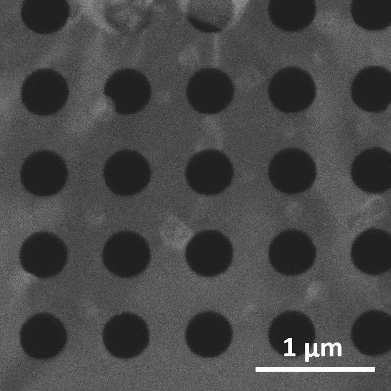
The sacrificial template is a thin silicon nitride membrane supported by a silicon frame. This structure more or less serves as the substrate on which the waveguide is constructed. An array of nanosized holes is then patterned into this membrane so that it can serve as a kind of template. At this point the tungsten disulfide crystal is pushed into the membrane. By sending ions through the membrane, the nanoholes create a pattern in the crystal. Finally, the silicon nitride membrane is etched away, leaving the tungsten disulfide crystal suspended in the silicon frame.
This periodic array of holes in the crystal also addresses another fundamental problem: measuring the performance of the waveguide mode. By their very nature, a waveguide directs light in the plane of the material. However, at this ultimate limit the researchers found that it was very difficult to distinguish the guided light from the light propagating freely in space. The array of holes scatters a small amount of light out of the plane of the material so it can be more easily detected.
While this device is the thinnest optical waveguide, reliably producing tungsten disulfide for large areas at high quality remains a challenge, potentially hindering these devices quickly finding their way into commercial optoelectronic devices.
Source: Spectrum


Levitra 20 Mg Online Cialis (Tadalafil)No Presciption Needed Canadian Pharmacy Generic Viagra [url=http://cialicheap.com]cialis canada[/url] What’S Better Penicillin Or Amoxicillin