We are consigning CMOS to the history books,” says SFN CEO David Summerland.

Bizen is a new semiconductor process that applies the principles of quantum tunnel mechanics to any computing or power technology.
Importantly, Bizen halves the number of process layers required. All this is achieved while equalling or bettering the speed and low power capabilities offered by current CMOS devices.
”Bizen has the ability to enable the UK to develop a leadership position in semiconductor manufacturing,” says Summerland.
Bizen technology lets designers create a simpler circuit with far fewer layers and increased logic density.
For example, the number of layers needed for a Bizen device range from four to eight for devices supporting low to high voltage operation, compared with ten to seventeen for CMOS. Using Bizen, power consumption drops, the size drops and the integration and speed increases, allowing complex devices to be manufactured in the large geometry fabs that exist in the UK.
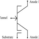
Bizen is essentially a pnp device whose base is driven through a quantum tunnelling junction, and which includes a second tunnelling junction to internally self-bias the transistor – more of the technology later. It is, said Summerland, starting out on silicon, but is capable of migrating to GaN and other compound semiconductors.
The transistor has a pnp-like structure, but with a difference at the base.
“It is a bipolar mechanism, not mono-polar like a mosfet,” said Summerland. “You don’t have direct contact to the base like a BJT, and it is not oxide-isolated like a mosfet. Instead there is a tunnelling junction to the base well with heavy doping and an abrupt junction. The result is Bizen – bipolar-zener – which retains the advantages of traditional bipolar processing yet removes the disadvantages by using Zener quantum tunnel mechanics.”
While the names ‘collector’ and ’emitter’ could have been used for the two non-tunnel (‘base’) electrodes, the device is symmetrical – those two terminals can be swapped without a functional change, according to SNF, so it has chosen to name them* ‘anode 1’ and ‘anode 2’.
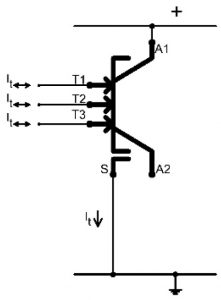
A second tunnelling junction, represented by two horizontal lines in the device diagram, biases the device so that it is ‘on’ (but not saturated) when the tunnel terminal is open-circuit. While this represents a continuous current flow to ground during operation, tunnel current is typically only 2-5nA, according to Summerland, who added that a lower-power ‘sleep’ mode can be introduced by including a single structure that can disconnect the bias tunnelling junctions of many – perhaps a thousand – bizen transistors from the negative rail.
 Bizen three-input NOR gate – this is current rather than voltage logic. Connect any input to the positive rail to stop conduction between anodes.
In this open-circuit condition, the tunnel electrode will float at 200-300mV below the most positive anode (see diagram left), and the device can pass 20-30nA between its anodes with a drop as low as a few millivolts across those anodes.
This enables one Bizen transistor to pull up ~10 tunnelling junctions of following Bizen transistors up to within millivolts of the positive rail -to use TTL parlance, it has a fan-out of ~10.
When the tunnelling connection of a device is pulled to the positive rail, the current path between its two anodes is turned off and the tunnel terminals of following devices are not driven – they are left to float.
As such, any logic built with Bizen transistors is current-based logic rather than voltage-based, and does not require space-wasting resistors or additional current sinks beyond the biasing tunnel junction.
The grant has been made by the ‘Driving the Electric Revolution Challenge’ program, part of UKRI’s Industrial Strategy Challenge Fund.
The aim of the initiative is to position the UK to seize the economic opportunities from the global transition to clean technologies and electrification, helping businesses across numerous sectors including transport, energy, construction and agriculture to invest and work together to capitalise on the UK’s strengths in this technology. SFN is one of more than 30 partner research and technology organisations that will collaborate in new Industrialisation Centres announced by the UK government.
Since mid-2018, SFN has been in collaboration with Semefab, the semiconductor and MEMS fab in Glenrothes, for process development and qualification leading to device production. First test chips are planned for this summer.
source; electronicweekly


